[讨论] SPI接口集中研究

xiaoxin1   2009-12-29 11:48 楼主
援引自http://embedded.com/columns/begi ... 83?_requestid=39340

Both SPI and I2C provide good support for communication with slow peripheral devices that are accessed intermittently. EEPROMs and real-time clocks are examples of such devices. But SPI is better suited than I2C for applications that are naturally thought of as data streams (as opposed to reading and writing addressed locations in a slave device). An example of a "stream" application is data communication between microprocessors or digital signal processors. Another is data transfer from analog-to-digital converters.

SPI can also achieve significantly higher data rates than I2C. SPI-compatible interfaces often range into the tens of megahertz. SPI really gains efficiency in applications that take advantage of its duplex capability, such as the communication between a "codec" (coder-decoder) and a digital signal processor, which consists of simultaneously sending samples in and out.

SPI devices communicate using a master-slave relationship. Due to its lack of built-in device addressing, SPI requires more effort and more hardware resources than I2C when more than one slave is involved. But SPI tends to be simpler and more efficient than I2C in point-to-point (single master, single slave) applications for the very same reason; the lack of device addressing means less overhead.

这里总结了SPI的几个主要特点:

- 比I2C更加适合处理数据流
- 比I2C更加高速
- 具有双工能力
- 缺少内置的寻址能力,所以支持多个slave不如I2C方便
- 一对一接口使用时非常简单

回复评论 (7)

援引自:http://en.wikipedia.org/wiki/Serial_Peripheral_Interface_Bus

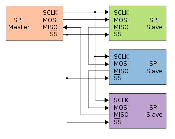
The SPI bus specifies four logic signals.

SCLK — Serial Clock (output from master)
MOSI/SIMO — Master Output, Slave Input (output from master)
MISO/SOMI — Master Input, Slave Output (output from slave)
SS — Slave Select (active low; output from master)
Alternative naming conventions are also widely used:

SCK, CLK — Serial Clock (output from master)
SDI, DI, SI — Serial Data In, Data In, Serial In
SDO, DO, SO — Serial Data Out, Data Out, Serial Out
nCS, CS, CSB, nSS, STE — Chip Select, Slave Transmit Enable (active low; output from master)
The SDI/SDO (DI/DO, SI/SO) convention requires that SDO on the master be connected to SDI on the slave, and vice-versa. Chip select polarity is rarely active high, although some notations (such as SS or CS instead of nSS or nCS) suggest otherwise.
SPI port pin names for particular IC products may differ from those depicted in these illustrations.
这里指出了SPI的四个接口信号:
- SCLK:这是同步的串行时钟
- MOSI:下行通道
- MISO:上行通道
- SS:片选信号
命名会有不同,但是万变不离其宗。
点赞  2009-12-29 11:48
The SPI bus can operate with a single master device and with one or more slave devices.
If a single slave device is used, the SS pin may be fixed to logic low if the slave permits it. Some slaves require the falling edge (high->low transition) of the slave select to initiate an action such as the MAX1242 by Maxim, an ADC, that starts conversion on said transition. With multiple slave devices, an independent SS signal is required from the master for each slave device.
Most slave devices have tri-state outputs so their MISO signal becomes high impedance ("disconnected") when the device is not selected. Devices without tristate outputs can't share SPI bus segments with other devices; only one such slave could talk to the master, and only its chip select could be activated.

这里提醒了多个slave情况下的配置方法:
- 为了支持多个slave,master装置必须有多个专用的片选信号一一控制slave
- 在多个slave的应用中,上行通道类似于总线共享,因此建议做成三态输出,避免多重驱动,这个和 I2C 有点类似
点赞  2009-12-29 11:49
援引自: http://en.wikipedia.org/wiki/Serial_Peripheral_Interface_Bus

To begin a communication, the master first configures the clock, using a frequency less than or equal to the maximum frequency the slave device supports. Such frequencies are commonly in the range of 1-70 MHz.
The master then pulls the slave select low for the desired chip. If a waiting period is required (such as for analog-to-digital conversion) then the master must wait for at least that period of time before starting to issue clock cycles.
During each SPI clock cycle, a full duplex data transmission occurs:
  • the master sends a bit on the MOSI line; the slave reads it from that same line
  • the slave sends a bit on the MISO line; the master reads it from that same line
Not all transmissions require all four of these operations to be meaningful but they do happen.
Every slave on the bus that hasn't been activated using its slave select line must disregard the input clock and MOSI signals, and must not drive MISO. The master must select only one slave at a time.
Transmissions may involve any number of clock cycles. When there is no more data to be transmitted, the master stops toggling its clock. Normally, it then deselects the slave.

数据传输大致分5步:
1. 配置所需时钟;
2. 片选从设备;
3. 等待必要的启动时间;
4. 开始数据传输周期;
5. 传输结束,关闭时钟和片选

根据CPOL和CPHA,一般制定出4种接口模式,如下所示

SPI-modeCPOLCPHA
0
1
2
3
0
0
1
1
0
1
0
1
Table 1: SPI Modes
点赞  2009-12-29 11:49
援引自:http://en.wikipedia.org/wiki/Serial_Peripheral_Interface_Bus

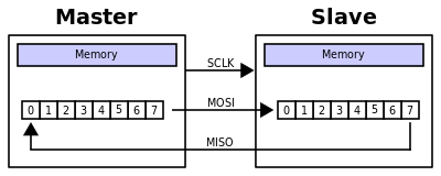
Transmissions normally involve two shift registers of some given word size, such as eight bits, one in the master and one in the slave; they are connected in a ring. Data is usually shifted out with the most significant bit first, while shifting a new least significant bit into the same register. After that register has been shifted out, the master and slave have exchanged register values. Then each device takes that value and does something with it, such as writing it to memory. If there is more data to exchange, the shift registers are loaded with new data and the process repeats.


Transmissions often consist of 8-bit words, and a master can initiate multiple such transmissions if it wishes/needs. However, other word sizes are also common, such as 16-bit words for touchscreen controllers or audio codecs, like the TSC2101 from Texas Instruments; or 12-bit words for many digital-to-analog or analog-to-digital converters.

SPI的实现,所需的资源,主要就是两个特定长度的移位寄存器,当然还有随后需要进一步存储的FIFO等等。
点赞  2009-12-29 11:50
援引自:http://en.wikipedia.org/wiki/Serial_Peripheral_Interface_Bus

In addition to setting the clock frequency, the master must also configure the clock polarity and phase with respect to the data. Freescale's SPI Block Guide [1] names these two options as CPOL and CPHA respectively, and most vendors have adopted that convention.


The timing diagram is shown to the right. The timing is further described below and applies to both the master and the slave device.
  • At CPOL=0 the base value of the clock is zero
    • For CPHA=0, data are read on the clock's rising edge (low->high transition) and data are changed on a falling edge (high->low clock transition).
    • For CPHA=1, data are read on the clock's falling edge and data are changed on a rising edge.
  • At CPOL=1 the base value of the clock is one (inversion of CPOL=0)
    • For CPHA=0, data are read on clock's falling edge and data are changed on a rising edge.
    • For CPHA=1, data are read on clock's rising edge and data are changed on a falling edge.
That is, CPHA=0 means sample on the leading (first) clock edge, while CPHA=1 means sample on the trailing (second) clock edge, regardless of whether that clock edge is rising or falling. Note that with CPHA=0, the data must be stable for a half cycle before the first clock cycle. For all CPOL and CPHA modes, the initial clock value must be stable before the chip select line goes active.
Also, note that "data are read" in this document more typically means "data may be read". The MOSI and MISO signals are usually stable (at their reception points) for the half cycle until the next clock transition. SPI master and slave devices may well sample data at different points in that half cycle.
This adds more flexibility to the communication channel between the master and slave.
Some products use different naming conventions. For example, the TI MSP430 uses the name UCCKPL instead of CPOL, and its UCCKPH is the inverse of CPHA. When connecting two chips together, carefully examine the clock phase initialization values to be sure of using the right settings.

时钟的配置要点:
- CPOL为0就是从0开始,从上升沿开始
- CPOL为1就是从1开始,从下降沿开始
- CPHA为0就是在leading edge抽样数据
- CPHA为1就是在trailing edge抽样数据
就是这么简单
点赞  2009-12-29 11:51
援引自: http://en.wikipedia.org/wiki/Serial_Peripheral_Interface_Bus

Some products with SPI bus are designed to be capable of being connected in a daisy chain configuration, the first slave output being connected to the second slave input, etc. The SPI port of each slave is designed to send out during the second group of clock pulses an exact copy of what it received during the first group of clock pulses. The whole chain acts as an SPI communication shift register; daisy chaining is often done with shift registers to provide a bank of inputs or outputs through SPI. Such a feature only requires a single SS line from the master, rather than a separate SS line for each slave.[2]
Applications (discussed later) that require a daisy chain configuration include SGPIO and JTAG.

点赞  2009-12-29 11:51
由于SPI是一个事实标准,各个公司的实现各不相同,这里我们一起来看一个例子。
这是Numonyx的Flash Memory——M25P32。放上PDF文件,大家一起来参详一下。
http://www.numonyx.com/Documents/Datasheets/M25P32.pdf
点赞  2009-12-29 11:51
电子工程世界版权所有 京B2-20211791 京ICP备10001474号-1 京公网安备 11010802033920号
    写回复